- 您现在的位置:买卖IC网 > Sheet目录2011 > MAX5856AECM+D (Maxim Integrated Products)IC DAC 8BIT DUAL 300MSPS 48-TQFP
MAX5856A
Dual 8-Bit, 300Msps DAC with 4x/2x/1x
Interpolation Filters and PLL
_______________________________________________________________________________________
3
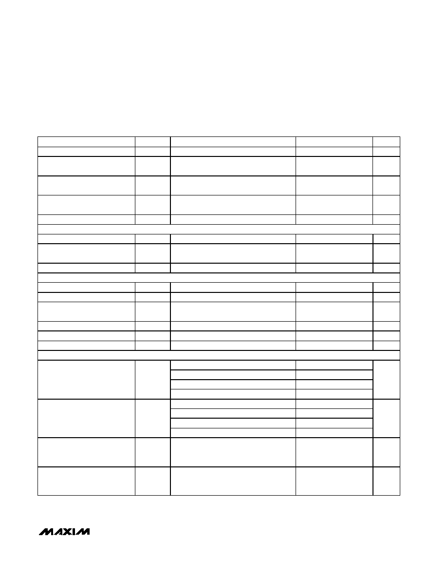
ELECTRICAL CHARACTERISTICS (continued)
(AVDD = DVDD = PVDD = 3V, AGND = DGND = PGND = 0, fDAC = 165Msps, no interpolation, PLL disabled, external reference,
VREFO = 1.2V, IFS = 20mA, output amplitude = 0dB FS, differential output, TA = TMIN to TMAX, unless otherwise noted. TA > +25°C,
guaranteed by production test. TA < +25°C, guaranteed by design and characterization. Typical values are at TA = +25°C.)
PARAMETER
SYMBOL
CONDITIONS
MIN
TYP
MAX
UNITS
Noise Spectral Density
nD
fDAC = 165Msps, fOUT = 5MHz
-133
dBm/Hz
Output Channel-to-Channel
Isolation
fOUT = 5MHz
80
dB
Gain Mismatch Between
Channels
fOUT = 5MHz
±0.05
dB
Phase Mismatch Between
Channels
fOUT = 5MHz
±0.15
Degrees
Wideband Output Noise
50
pA/
√Hz
ANALOG OUTPUT
Full-Scale Output Current Range
IFS
220
mA
Output Voltage Compliance
Range
-1.0
+1.25
V
Output Leakage Current
Power-down or standby mode
-5
+5
A
REFERENCE
Reference Output Voltage
VREFO
REN = AGND
1.14
1.24
1.34
V
Output-Voltage Temperature Drift
TCVREF
±50
ppm/
°C
Reference Output Drive
Capability
50
A
Reference Input Voltage Range
REN = AVDD
0.1
1.32
V
Reference Supply Rejection
0.2
mV/V
Current Gain
IFS/IREF
32
mA/mA
INTERPOLATION FILTER (2x interpolation)
-0.005dB
0.398
-0.01dB
0.402
-0.1dB
0.419
Passband Width
fOUT/
0.5fDAC
-3dB
0.478
MHz/
MHz
0.604fDAC / 2 to 1.396fDAC / 2
74
0.600fDAC / 2 to 1.400fDAC / 2
62
0.594fDAC / 2 to 1.406fDAC / 2
53
Stopband Rejection
0.532fDAC / 2 to 1.468fDAC / 2
14
dB
Group Delay
18
Data
clock
cycles
Impulse Response Duration
22
Data
clock
cycles
发布紧急采购,3分钟左右您将得到回复。
相关PDF资料
MAX5858AECM+D
IC DAC 10BIT DUAL 300MSPS 48TQFP
MAX5858ECM+D
IC DAC 10BIT DUAL 300MSPS 48TQFP
MAX5863ETM+T
IC AFE 8/10BIT 7.5MSPS 48-TQFN
MAX5864ETM+T
IC ANLG FRONT END 22MSPS 48-TQFN
MAX5865ETM+T
IC ANLG FRONT END 40MSPS 48-TQFN
MAX5866ETM+
IC ANLG FRONT END 60MSPS 48-TQFN
MAX5873EGK+D
IC DAC 12BIT 200MSPS DUAL 68-QFN
MAX5874EGK+D
IC DAC 14BIT 200MSPS DUAL 68-QFN
相关代理商/技术参数
MAX5856AECM+TD
功能描述:数模转换器- DAC 8-Bit 2Ch 300Msps DAC RoHS:否 制造商:Texas Instruments 转换器数量:1 DAC 输出端数量:1 转换速率:2 MSPs 分辨率:16 bit 接口类型:QSPI, SPI, Serial (3-Wire, Microwire) 稳定时间:1 us 最大工作温度:+ 85 C 安装风格:SMD/SMT 封装 / 箱体:SOIC-14 封装:Tube
MAX5856AECM-D
功能描述:数模转换器- DAC RoHS:否 制造商:Texas Instruments 转换器数量:1 DAC 输出端数量:1 转换速率:2 MSPs 分辨率:16 bit 接口类型:QSPI, SPI, Serial (3-Wire, Microwire) 稳定时间:1 us 最大工作温度:+ 85 C 安装风格:SMD/SMT 封装 / 箱体:SOIC-14 封装:Tube
MAX5856AECM-TD
功能描述:数模转换器- DAC RoHS:否 制造商:Texas Instruments 转换器数量:1 DAC 输出端数量:1 转换速率:2 MSPs 分辨率:16 bit 接口类型:QSPI, SPI, Serial (3-Wire, Microwire) 稳定时间:1 us 最大工作温度:+ 85 C 安装风格:SMD/SMT 封装 / 箱体:SOIC-14 封装:Tube
MAX5858AECM
制造商:Rochester Electronics LLC 功能描述: 制造商:Maxim Integrated Products 功能描述:
MAX5858AECM+D
功能描述:数模转换器- DAC 10-Bit 2Ch 300Msps DAC RoHS:否 制造商:Texas Instruments 转换器数量:1 DAC 输出端数量:1 转换速率:2 MSPs 分辨率:16 bit 接口类型:QSPI, SPI, Serial (3-Wire, Microwire) 稳定时间:1 us 最大工作温度:+ 85 C 安装风格:SMD/SMT 封装 / 箱体:SOIC-14 封装:Tube
MAX5858AECM+TD
功能描述:数模转换器- DAC 10-Bit 2Ch 300Msps DAC RoHS:否 制造商:Texas Instruments 转换器数量:1 DAC 输出端数量:1 转换速率:2 MSPs 分辨率:16 bit 接口类型:QSPI, SPI, Serial (3-Wire, Microwire) 稳定时间:1 us 最大工作温度:+ 85 C 安装风格:SMD/SMT 封装 / 箱体:SOIC-14 封装:Tube
MAX5858AECM-D
功能描述:数模转换器- DAC RoHS:否 制造商:Texas Instruments 转换器数量:1 DAC 输出端数量:1 转换速率:2 MSPs 分辨率:16 bit 接口类型:QSPI, SPI, Serial (3-Wire, Microwire) 稳定时间:1 us 最大工作温度:+ 85 C 安装风格:SMD/SMT 封装 / 箱体:SOIC-14 封装:Tube
MAX5858AECM-TD
功能描述:数模转换器- DAC RoHS:否 制造商:Texas Instruments 转换器数量:1 DAC 输出端数量:1 转换速率:2 MSPs 分辨率:16 bit 接口类型:QSPI, SPI, Serial (3-Wire, Microwire) 稳定时间:1 us 最大工作温度:+ 85 C 安装风格:SMD/SMT 封装 / 箱体:SOIC-14 封装:Tube